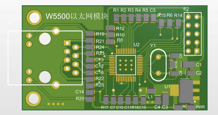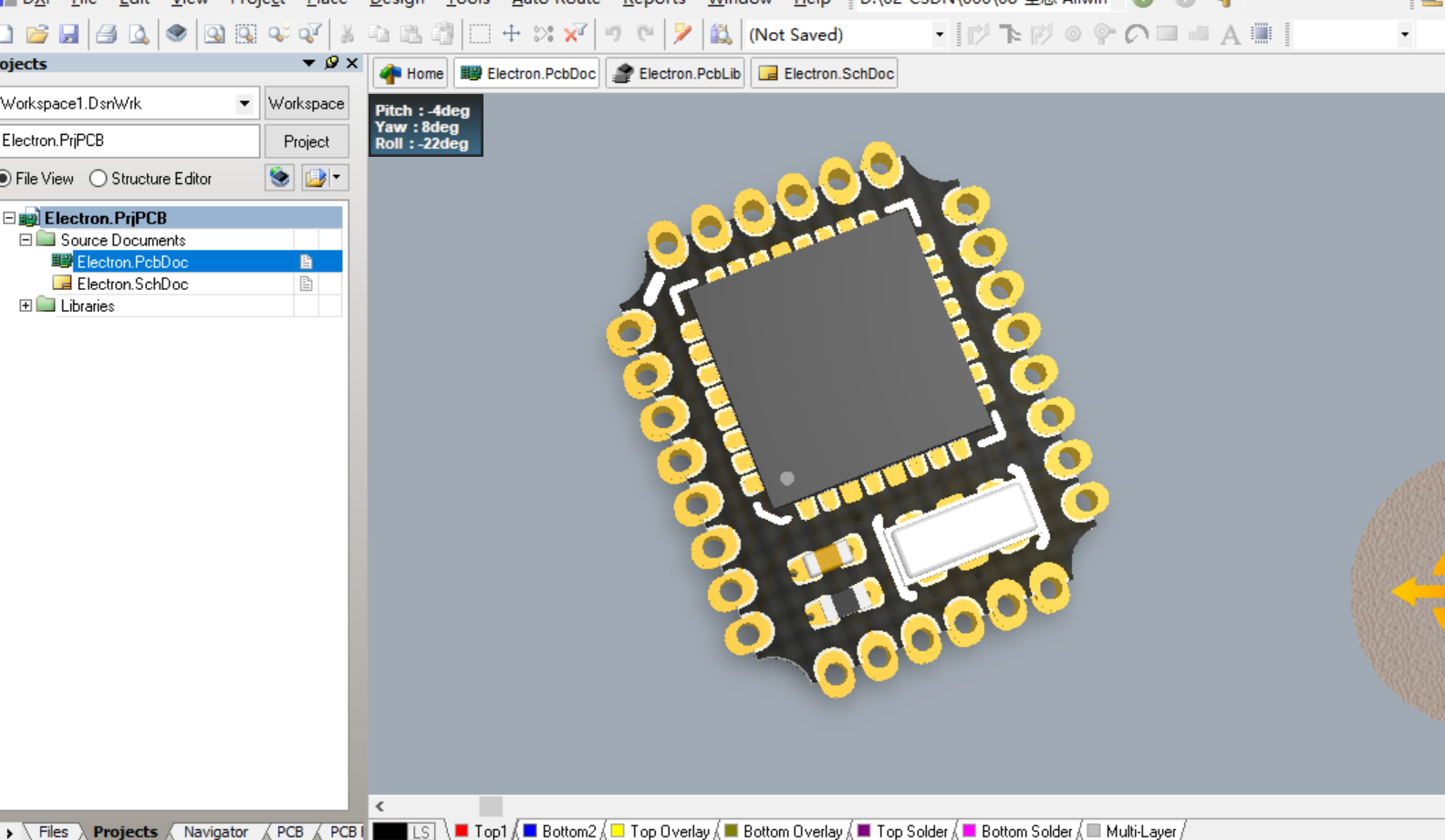
Good CADs for PCB design allow to re-annotate designators at PCB-level. You can spend even minutes looking for the right place of a given component, and often you need to rotate too many times the board, running the risk to throw away already placed components. But if you are going to assemble a prototype manually (I'm used to assemble manually even boards with 3-400 components, believe it or not), then having all component designators scattered on the board is a hell.

This is not a critical aspect if the board will be assembled using a pick-and-place (modern pick-and-places are able to process pick-and-place files that contain the exact coordinates of a given component on a board) or if it contains few tens of components.

This happens because often the development of schematics isn't linear, especially if we are designing some sub-modules before others or if we are reusing some schematics sheets from other and well-tested designs.

R1 is somewhere, R2 is hidden in another place, and so on. It's really common that at the end of the board layout we have that all component designators are randomly scattered over the board.


 0 kommentar(er)
